Printed Circuit Boards & Micro-Electronics Assembly

High-density microelectronics assembly for medical devices
Tightly integrated circuitry
for space-constrained systems
Printed circuit boards and micro-electronics assemblies form the neural network of modern medical devices, routing power, data, and therapy signals through sub-millimeter channels while surviving sterilization, shock, and decades inside the body. High-density interconnect (HDI) layers, rigid-flex stack-ups, and chip-on-board techniques let engineers shrink form factors without sacrificing signal integrity.
Whether the goal is a brain computer interface, neuromodulator, wearable sensor, or point-of-care diagnostic, precision-built boards and assemblies shorten paths from concept to clinic by uniting sensing, control, and wireless functions in a single, qualified module.
Our PCBA & Microelectronics Capabilities
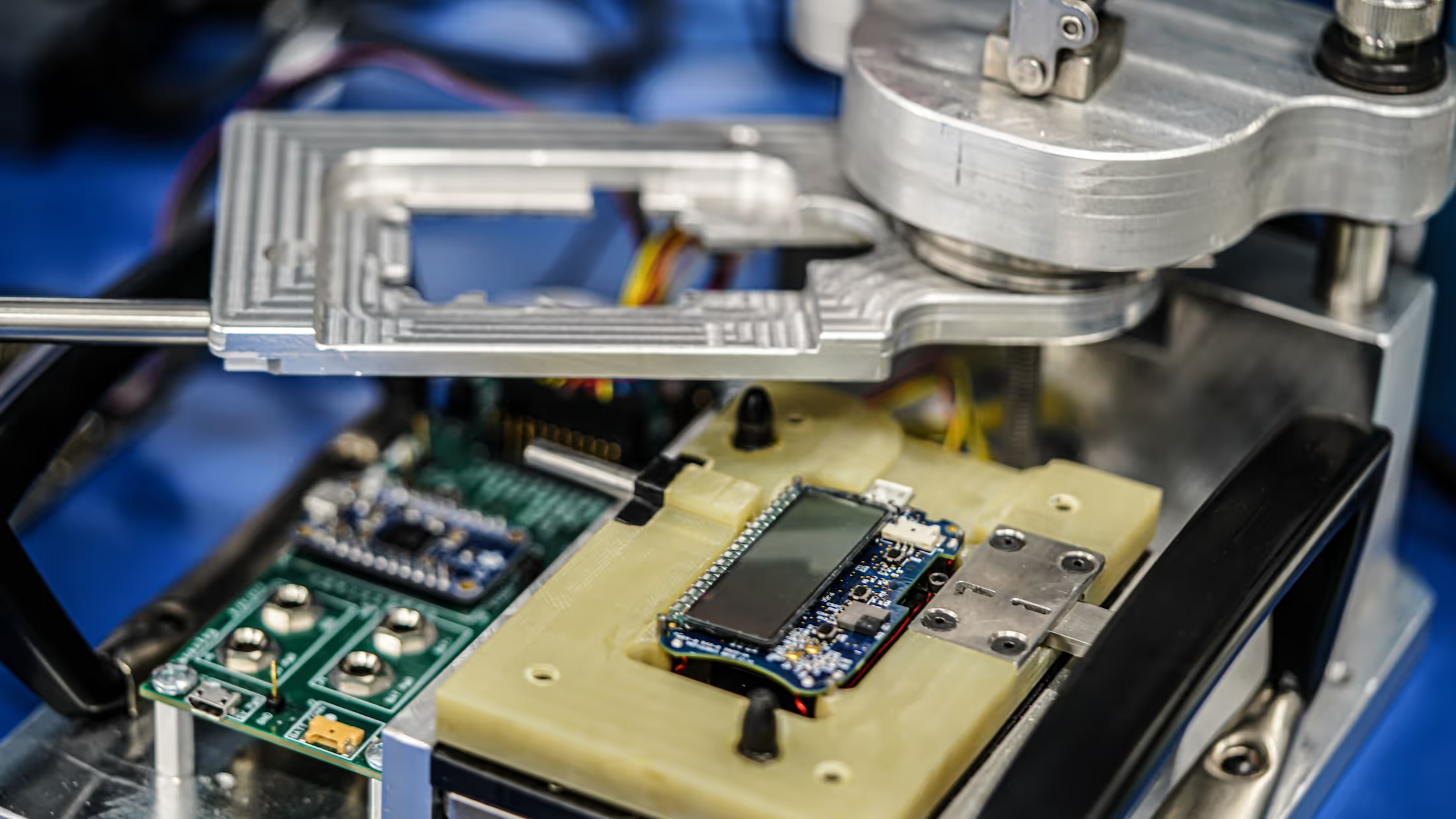
Cirtec combines advanced substrates, ultra-fine features, and class-controlled assembly to deliver implant-ready electronics.
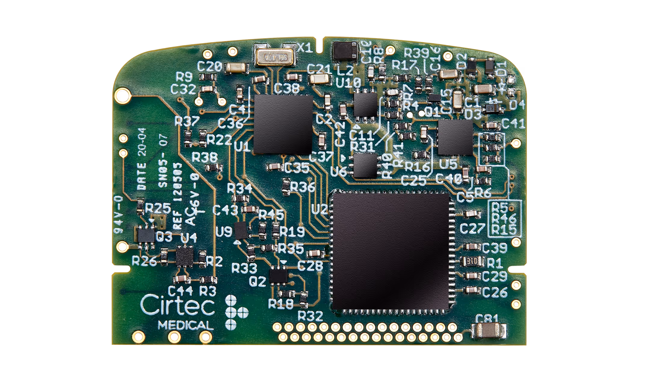
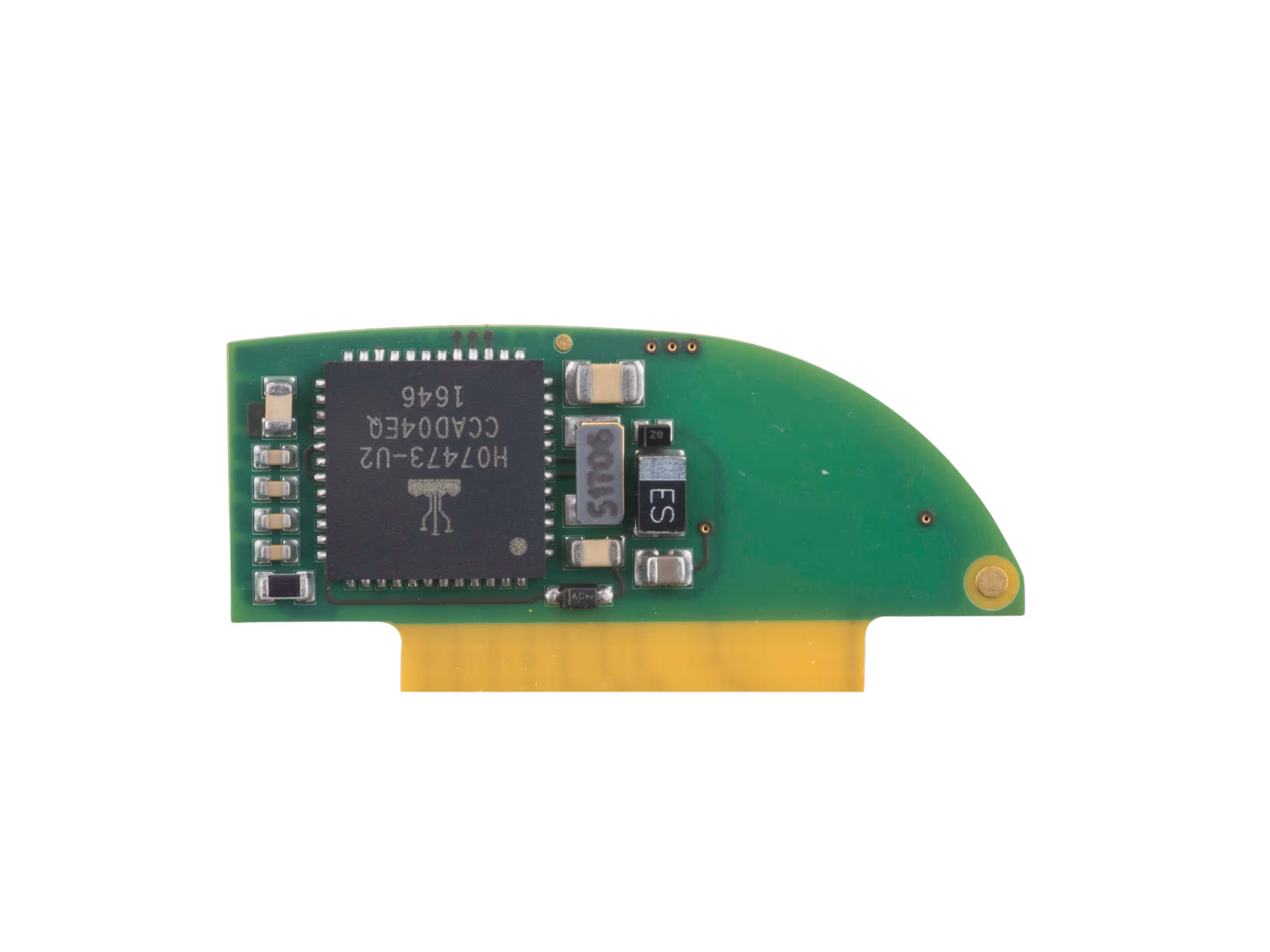
4–10 layer HDI stack-ups, microvias, and rigid-flex constructions route high-speed signals through tight bends while eliminating bulky connectors, ideal for pulse generators, cochlear implants, and wearables.
Additive thin-film lines/spaces down to 3 µm and vias to 25 µm enable unmatched channel density on polyimide or alumina substrates for neural and biosensor arrays . Standard flex circuits reach 5 µm lines for cost-effective volume builds.
Class 7 and 8 cleanrooms place 0201 passives, 0.3 mm µBGAs, flip-chips, wire-bonds, and epoxy-backfilled ASICs under one roof, backed by ESD-safe workflows and hermetic sealing capability for active implants.
3-D AOI, X-ray, functional burn-in, and ISO 13485 traceability ensure every board meets IPC Class III, IEC 60601, and implantable-device reliability targets. Cleanroom photolithography and helium-leak screening are available for ultra-critical builds.
Why Choose Cirtecfor Printed Circuit Boards & Micro Electronics Assembly?
- Micron-scale circuit density
- Class 7 and 8 cleanrooms
- HDI rigid-flex expertise
- ISO 13485 traceability
- Prototype-to-volume automation
Cirtec unites HDI PCB layout, thin-film fabrication, SMT, and micro-assembly inside a vertically integrated, ISO 13485-certified network. Our engineers co-develop boards with ASIC, sensor, and hermetic-package teams, compressing design-for-manufacture and regulatory documentation into a single sprint.
Rapid-turn prototype lines mirror our automated volume equipment, so performance proven on Day 1 scales to millions of units without re-qualification. In-house X-ray, HALT/HASS, and helium-leak labs de-risk longevity freeing R&D teams to push what’s possible, not paperwork.
Integrate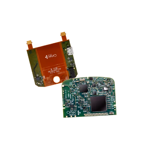 PCBAs
PCBAs
and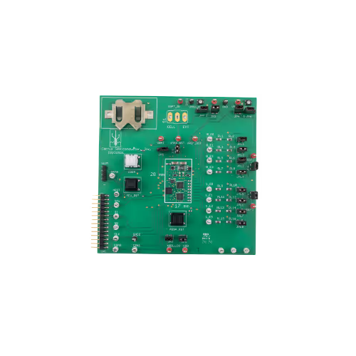 microelectronics
with confidence.avif)
Connect with our team to get started